
Pan Yongjing
Year 4 Electrical Engineering
A0257283X
Contents page
1.4 Specifications and Constraints 3
1.5 Novelty and Contributions 3
2. Background and Literature Review 4
3.2 Key Antenna Performance Metrics 4
3.3 Selection of planar antenna type 5
3.3.1 Concept evaluation matrix 6
3.3.2 Mitigating the Disadvantages of Patch Antenna 6
3.3.3. Preliminary feasibility calculations 7
3.4 Selection of type of circularly-polarised patch antenna 7
3.4.1 How the Circularly-Polarised Patch Antenna Works 7
3.5 Substrate material and height selection 10
4.1 Prototype 1: Optimising single patch 11
4.2 Prototype 2: Optimising 2x2 array (circular_array_3) 12
4.3 Prototype 3: Order of sequential rotation investigation 14
4.4 Prototype 4: 2x4 Array Simulation 15
4.5 Prototype 5: Feed network design 16
4.6 Prototype 6: PCB1 Feed network 17
6. Conclusion & Future Works 19
1. Introduction
This project focuses on developing a custom space-based Ku-band antenna for the Galassia 5 (G5)’s unique requirements.
1.2 Problem Statement
As mentioned in the introduction to G5, the team discovered that there is no existing commercial space-qualified Ku-band communication hardware meeting our frequency requirements (13.93-13.99 GHz). The space-based Ku antenna is one crucial part of the system that together with the Ku-band upconverter and ground station, form the custom-designed communication link from the satellite to the ground station. Specifically, the antenna serves to amplify and transmit signals from the satellite to the ground station. Hence, there is a need to develop a custom Ku antenna meeting the G5 mission requirements.
1.3 Objectives and Scope
To design, prototype and test an antenna operating in the required frequency range of 13.93-13.99GHz for space-based application.
1.4 Specifications and Constraints
- Frequency range: 13.93-13.99 GHz
- Central frequency: 13.95 GHz
- Maximum size: 100mm x 100mm x 4.26 mm
- Minimum gain: 10dBi
- Minimum beamwidth: 24 degrees
The central frequency, gain and beamwidth were set by the team lead-cum-system engineer. From discussions with the mechanical team, the mounting of the antenna was determined to be on a 1U (10cmx10cm) face of the CubeSat. Similar to Gomspace’s S-band antenna ANT2150 (lit), the mounting screws will be at 4 corners of the 1U face. A minimum distance of 1cm from the face edges is set for mechanical stability. Factoring in the antenna’s radiating elements will need ~0.3 wavelength (depends on antenna substrate to be chosen) separation from metal, this gives maximum space for the antenna’s radiating elements.
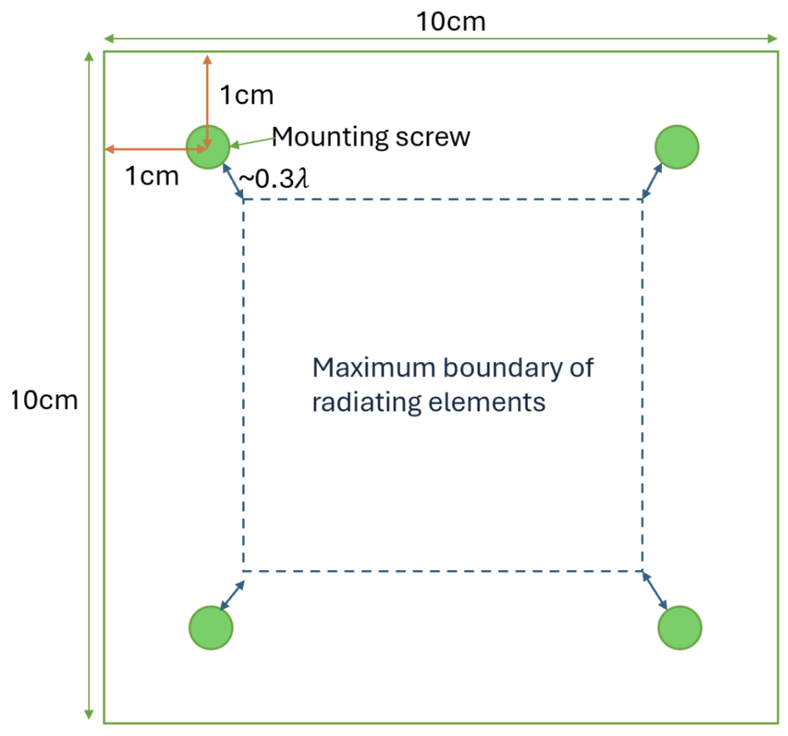
Figure 1. Maximum boundary of radiating element (assuming rectangular boundary)
1.5 Novelty and Contributions
As mentioned in G5’s introduction, existing communication systems do not operate in the narrow, specific frequency range of 13.93-13.99 GHz. The design of a custom Ku antenna to meet our mission’s requirements hence addresses this gap in existing commercially-available space-based Ku-band antennae.
2. Background and Literature Review
To implement communications within the physical limits of a CubeSat, planar antennas - such as microstrip patches and slots - are an optimal choice due to their low profile, low cost, and ease of integration with microwave circuits (Tubbal et al., 2015). Unlike deployable reflector or helical antennas, planar antennas do not require complex deployment mechanisms and occupy significantly less real estate on the satellite body (Tubbal et al., 2015). These properties make them uniquely suited to meet the tight sub-4.6mm thickness constraints of the G5 mission.
Despite their physical suitability, creating highly miniaturised planar antennas that maintain acceptable bandwidth and radiation efficiency remains extremely challenging (Zhang, 2011). There is a fundamental trade-off in antenna design: because an antenna’s gain is closely related to its physical aperture, miniaturisation tends to reduce overall gain (Zhu & Liu, 2025). Additionally, the fundamental challenge of designing a compact antenna is a reduced bandwidth caused by a high Q factor (Hossain, 2023).
To compensate for the low gain of miniaturized elements, multiple microstrip patches are typically combined to form an array.
3. Design Methodology
3.1 Antenna Design Process
To meet mission deliverables, a systematic methodology was employed: requirement definition, EM simulation, prototyping, and testing. A simulation-first approach was adopted using ANSYS HFSS to identify flaws before manufacturing. The Finite Element Method (FEM) was selected over MoM or FDTD due to its superior flexibility in modelling complex 3D structures and multi-port setups (MacroFab, n.d.;Intrasensors, 2024).
3.2 Key Antenna Performance Metrics
The antenna’s performance is primarily characterised by S11 (Return Loss), where a value of -10 dB ensures that over 90% of source energy is successfully delivered to the patches within the 13.93-13.99 GHz operational range (Verwilligen, 2015). To maintain link stability against Faraday rotation and CubeSat misalignment, the design utilises Right-Hand Circular Polarisation (RHCP) (Tubbal et al., 2021). The design prioritises Realised RHCP Gain ($\ge10$ dBi), as this metric accounts for internal dielectric losses, impedance mismatch, and polarisation mismatch (Zvolensky, 2022). For this report, “gain” will always refer to realised RHCP gain. Coverage requirements are further defined by the Half-Power Beamwidth (HPBW), which necessitates a gain of -7 dBi at +-12 degrees. Finally, the Axial Ratio (AR) is maintained below 3 dB to ensure high-quality polarisation purity and to minimise energy waste through unwanted cross-polarisation (Abulgasem et al., 2021). For detailed explanations of the metrics, see Appendix x.
3.3 Selection of planar antenna type
3.3.1 Concept evaluation matrix
In various CubeSat antennae review papers, the most common types of planar antennae were patch antennae, followed by slot antennae and metasurface antennae (Gurbet & Doğu, 2025; Tubbal et al., 2015). A total of 4 factors were considered for selection of the best design:
- Availability of formulae
- Simplicity of design for circular polarisation
- Space heritage
- Ease of manufacturing
| Antenna type | Availability of design formulae | Simplicity of design for circular polarisation | Space heritage | Ease of manufacturing | Total |
|---|---|---|---|---|---|
| Patch antenna | 3 | 3 | 3 | 3 | 12 |
| Slot antenna | 2 | 1 | 1 | 2 | 6 |
| Metasurface antenna | 1 | 1 | 1 | 1 | 4 |
Table 1: Selection of antenna type
Using the evaluation matrix, patch antenna scores highest out of all factors considered and is hence chosen. This choice was also recommended early by both NUS and DSO mentors. Circularly polarised patch antennas are extensively studied, with abundant formulae and well-validated design methods available in literature (Balanis, 1997). Patch antennae are also widely used in CubeSats (Gurbet & Doğu, 2025; Silva et al., 2021; Veera & Ajay, 2025) and can be easily manufactured via PCB manufacturing.
In contrast, slot antennas and metasurface antennas are less commonly used in space systems. Achieving circular polarisation with slot antennas typically requires more complex geometries, while metasurfaces heavily rely on full-wave simulations [5] for beam steering and polarisation control. Furthermore, manufacturing metasurface antennas can be highly complex as it requires intricate sub-wavelength patterning and strict fabrication tolerances (Saeidi & Karamzadeh, 2025).
3.3.2 Mitigating the Disadvantages of Patch Antenna
Limited Gain: A single patch antenna generally has limited gain (Mohamadzade et al., 2020). However, this can be mitigated at high frequencies such as the Ku-band, where individual patch elements are physically small, enabling the creation of high-gain arrays without exceeding size constraints.
Narrowband: Patch antennas are inherently narrowband due to their resonant nature and high Q-factor (Hossain, 2023). However, our mission’s bandwidth requirement is already very narrow (0.06 GHz), thus this limitation is not critical.
Mutual Coupling: When grouping multiple patches to form a high-gain array, the close proximity of the elements introduces mutual coupling, which can lower antenna efficiency, cause impedance mismatching, and distort the radiation pattern (Li et al., 2018). This will be mitigated by ensuring adequate electrical spacing between the elements and optimising the feed network.
3.3.3. Preliminary feasibility calculations
The calculations for patch geometry require us to first select the dielectric substrate, r as this affects the guided wavelength g which determines the patch size. Considering standard PCB manufacturing for ease of fabrication, air substrate will not be considered, thus the minimum value is taken to be 1.96 of the Rogers RT/duroid 5880LZ substrate (Coonrod, 2010), giving us an upper limit of 15.35mm for g.
For conventional patch geometries, their fundamental dimensions are primarily dictated by the half-wavelength resonance within the dielectric substrate (Jackson, n.d.). For rectangular patches, the estimated size based on formulae [7] of one Ku-band patch element is about 7 mm x 5.2 mm. For a circular patch operating in its dominant TM11 mode, with radius of 0.293g, the diameter is about 7.6mm (“A TM31 Mode Circular Microstrip Patch Antenna”, n.d.). Taking the larger dimension of 7.6mm, and adding 10% margin to account for other geometric variations, we assume a 8.36x8.36mm patch.
One patch can achieve ~3-4 dBi of gain. By doubling the number of elements three times (each doubling theoretically increases gain by 3 dBi), a gain of ~12 dBi can be achieved with a 2x4 array. In the array, maintaining a separation of half a wavelength (~7.67 mm) between each element is recommended to prevent severe mutual coupling and grating lobes (Minz, Kang, & Park, 2020). Considering the required electrical separation from surrounding metal to avoid detuning, the antenna must be placed ~6.5 mm away from metallic mounting screws (Li et al., 2018). Including the electrical separation, the boundary is at 69.45x69.45mm, leaving 20mm of space for the mounting screws which is more than enough. Hence, a microstrip patch array easily fits within the physical constraints of the CubeSat, making it a highly viable solution for our specifications.
3.4 Selection of type of circularly-polarised patch antenna
A basic patch requires a patch layer, substrate, and ground plane (see Appendix x for details).
However, the 2x2 array necessitates a complex feed network to provide 90-degree phase shifts. Implementing this on the patch layer would cause spurious radiation and degrade S11. Consequently, a three-layer probe-fed design was chosen. A microstrip-line feed network was selected over stripline to simplify manufacturing and reduce transmission losses associated with multi-layer fabrication.
There are 3 main techniques. The first is a compact approach utilising a single-point feed combined with deliberate geometric perturbations - such as truncating the opposing corners of a square patch or introducing asymmetrical slots. The second is a dual-feed approach, which employs an external power divider network to feed two orthogonal edges of the patch with the required phase shift. These structural modifications intentionally detune the degenerate modes of the symmetrical patch. This forces the fundamental mode to split into two orthogonal components that naturally achieve the necessary in-phase quadrature (90-degree phase shift) required to radiate circularly polarised waves (Helit Team, n.d.; Orban & Moernaut, 2005). The third technique is to make a sequentially-rotated 2x2 array of a linearly-polarised single patch. In this technique, four elements in a 2x2 array are physically rotated and excited with sequential phase shifts of 0°, 90°, 180°, and 270° (Kuhlmann, 2023) (Fig x).
Figure 4. Circularly-Polarised Patch Concepts: a) Truncated corner patch, b) Dual-feed patch with Wilkinson Power Divider, c) Circular patch array
| Antenna Type | Gain | Simplicity of Design | Space Heritage | Total |
|---|---|---|---|---|
| Truncated Square Patch (CP) | 1 | 3 | 2 | 6 |
| Dual-Feed Rectangular Patch + Wilkinson Power Divider | 3 | 1 | 3 | 7 |
| Circular Probe-Fed Patch Array | 3 | 2 | 3 | 8 |
Table 2: Selection of patch antenna design
Among the three designs considered, the truncated square patch was eliminated early due to its inherently lower gain [8], also as highlighted by DSO mentors. The dual-feed rectangular patch can achieve good circular polarisation, but it requires a more complex feed structure per patch involving a Wilkinson power divider [9] and precise phase balancing. Such dual-feed implementations suffer from a significant increase in required surface area, making them very difficult to implement in a tightly spaced array (Christopher et al., 2004).
Being made of linearly polarised parts, the circular probe-fed patch array is low complexity while maintaining high gain and strong space heritage. This design is also supported by my NUS mentor. Therefore, the circular probe-fed patch antenna was selected.
Figure 5. Circularly-Polarised Patch Array Concepts: (left) Sequentially rotated array of circular patches from CST Design Suite and (right) AR of n-element arrays (Kuhlmann, 2023)
3.4 PCB Stackup Design
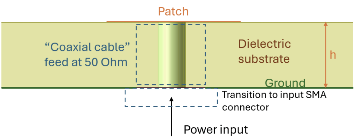
As mentioned in 3.4.1, a basic patch antenna consists of a patch layer, substrate and ground plane. As the circular patches are probe-fed (Fig. x), as compared to Fig. x, the feed is a via going through the substrate to contact the patch (Sowmya et al., 2012). For a singular patch, such a design (Fig. x) would be sufficient.
However, to create the 2x2 array, we need to excite each of 4 patches at 90 degrees phase difference which requires a feed network. If a complex feeding network were implemented on the same layer as the patches, it would generate undesired spurious radiation, which could affect the antenna’s overall performance and S11 (Minz, Kang, & Park, 2020). Thus, also accounting for the probe-fed design, a feed network must be designed on a 3rd layer. There are two options. It can either be a microstrip line or a stripline. A stripline is a signal trace sandwiched symmetrically between two substrate layers and two ground planes (Fig. x) (“A comparative study”, 2016). From my research, stripline would cause more losses so it was rejected. While this fully enclosed structure prevents radiation leakage, striplines can introduce higher losses (“A comparative study”, 2016). Furthermore, a stripline requires a more complex, heavier multi-layer fabrication process. Therefore, to minimise these transmission losses and simplify manufacturing, the microstrip line feed network was chosen instead.
3.5 Substrate material and height selection
The next step is to select the substrate material and heights, as these would affect the patch size and feed network trace widths.
3.5.1 Upper substrate & Substrate material
The selection of the substrate material and its height is important to antenna performance and mechanical integrity (Paul et al., 2015). Increasing the substrate thickness generally increases the bandwidth, which is highly desirable for ensuring a robust communication link (AL-Oqla & Omar, 2015). However, increasing this thickness also causes the resonance frequency to decrease and shift away from the intended target, whilst simultaneously decreasing the required physical dimensions of the antenna patch (Paul et al., 2015).
The choice of substrate material determines the relative dielectric constant r and the mechanical strength of the antenna. As dielectric constant increases, the guided wavelength decreases leading to a smaller antenna footprint (AL-Oqla & Omar, 2015). However, a high dielectric constant can increase undesirable surface waves, which causes significant power losses (AL-Oqla & Omar, 2015). Furthermore, mechanical reliability is paramount for CubeSat applications. A primary purpose of the substrate is to provide mechanical support to the etched electrical conductors (AL-Oqla & Omar, 2015). Substrates vary greatly in their mechanical firmness; some are brittle, whilst others are much more rigid (AL-Oqla & Omar, 2015).
When evaluating materials for the Ku-band CubeSat patch antenna, high-dielectric materials like FR-4 are first eliminated as they cause measurable decrease in directivity, gain, and bandwidth (Paul et al., 2015). Furthermore, FR-4 possesses a higher loss tangent, which indicates that a greater amount of current is leaked into the dielectric, thereby worsening the operational performance of the circuit (AL-Oqla & Omar, 2015). Consequently, although FR-4 is low cost, it is a poor option compared to advanced high-frequency laminates which we discuss next (AL-Oqla & Omar, 2015)
Rogers RO4350B (r = 3.66) was assessed against RT/duroid 5880 (r = 2.2). Whilst RT/duroid 5880 offers a low dielectric constant, it is a PTFE-based composite (Rogers Corporation, n.d.). Consequently, RT/duroid 5880 is inherently flexible and prone to deformation under stress. RO4350B was evaluated to be vastly superior because it does not deform, providing the rigid, mechanically firm structure required to withstand the harsh vibrations of a satellite launch.
Considering all these factors - balancing bandwidth requirements, size constraints, and the crucial need for mechanical rigidity - a substrate height of 0.762 mm and Rogers 4350B were selected, a decision also endorsed by my mentor.
3.5.2 Lower substrate height
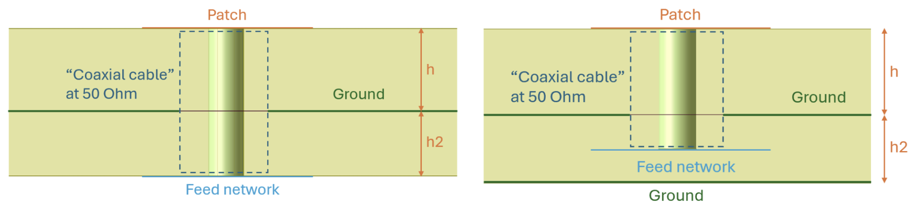
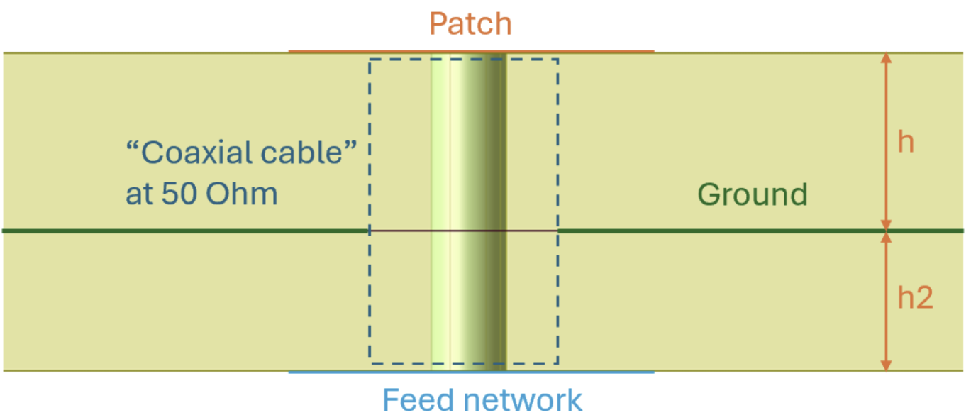
For the lower substrate height h2, this will be similar to h to reduce PCB warping, as unequal dielectric thicknesses can induce mechanical stress during lamination, leading to severe board deformation (Adrian, 2025; Cadence PCB Education, 2025). h2 will affect the trace widths of the feed network. The feed network will consist of 50 Ohm, 70.7 Ohm quarter-wave transformers and possibly lower impedances, due to the need to split the power source to 4 feeds or more. Due to the small area of the patches, the feed positions will also be close together, which means the feed network would need to be compact and thus the trace widths cannot be too wide, as it would lead to field leakage and coupling to neighbouring traces or feed points. The widths must also not be too small to introduce large manufacturing tolerance errors. Thus, h2 will be further tuned after more simulation.
4. Prototype Development
Antenna prototypes are developed via iterative simulations in HFSS, where each component e.g. patch, subarray, feed section are individually simulated, then combined to a bigger component and simulated again. Key metrics (3.1) are evaluated for each simulation, then modifications or parameter tunings are done to optimise the metrics further.
4.1 Prototype 1: Optimising single patch
This prototype aims to optimise S11 for a single patch. This helps create a good foundation for the overall S11 as many factors such as substrate permittivity variations, fabrication tolerances, and connector soldering can create impedance shifts leading to power reflection. To achieve good matching, the patch radius Rp and feed position Sf (Fig x) were tuned.
Using parametric sweep, the best Rp and Sf parameters (Table x) were respectively 3.092mm and 0.931mm, producing a lowest possible S11 minimum of -51 dB at 13.95 GHz. Designing the patch to achieve a deep null below -30 dB provides a generous design margin to absorb any frequency shifts caused by the previously mentioned manufacturing tolerances.
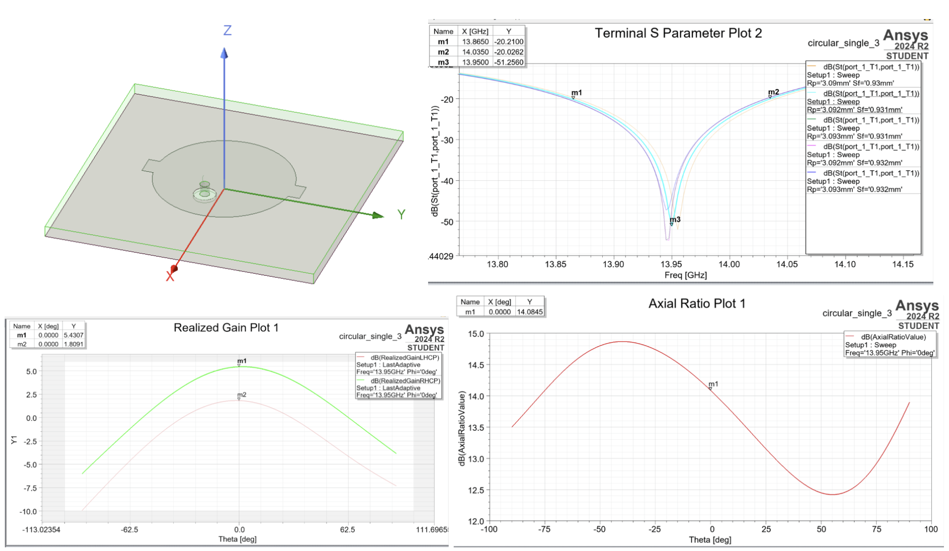
Figure 6. Performance of single patch (Prototype 1): a) Patch geometry, b) S11, c) Realised Gain, d) Axial Ratio
| Metrics | Best achieved metric | Parameter | Optimised parameter / mm |
|---|---|---|---|
| S11 | -51.25 dB | R_p | 3.092 |
| Realised RHCP Gain | 5.43 dBi | S_f | 0.931 |
| AR | 14.08 dB |
Table 3: Single Patch Optimization Metrics (Prototype 1)
A very high axial ratio of 14 dB is observed, as expected, as this single patch is linearly polarised.
4.2 Prototype 2: Optimising 2x2 array
This prototype forms a 2x2 array of the optimised single patch. As mentioned, the feeds are excited at different phases: from top left, clockwise at 0, 90, 180, 270 deg (Kuhlmann, 2023). The expected gain is 5.43 + 6 = 11.43 dBi.
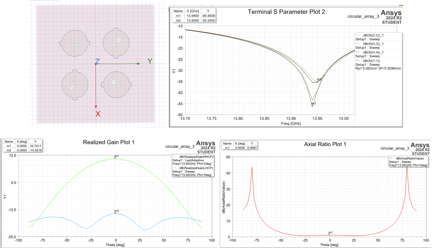
Figure 7. Performance of 2x2 Array (Prototype 2): a) Array geometry, b) S11 optimisation (before vs after), c) Realised Gain, d) Axial Ratio
| Metrics (boresight at 13.95 GHz) | Best achieved metric | Parameter | Optimised parameter / mm |
|---|---|---|---|
| S11 | -35.5 dB | R_p | 3.082 |
| Realised RHCP Gain | 10.74 dBi | S_f | 0.9296 |
| AR | 0.96 dB |
Table 4: 2x2 Array Optimization Metrics (Prototype 2)
Expanding the single patch into an array shifted the S11 minimum to a lower frequency than 13.95 GHz. This is a well-documented phenomenon caused by mutual coupling. Placing the elements in close proximity introduces adjacent structures that alter the fringing fields and interact with the effective input impedance of each patch, consequently shifting its natural resonant frequency (MathWorks, n.d.; Ray et al., 2008). Hence, R_p and S_f were re-tuned to centre the resonance at 13.95 GHz.
The gain of 10.74 dBi is slightly lower than the theoretical 11.43 dBi. This is also due to the mutual coupling between adjacent patches, which lowers overall antenna efficiency and causes slight deviations in the ideal radiation pattern that prevent perfect constructive interference (Li et al., 2018).
Validating Kuhlmann’s theory, the sequentially rotated array, through 90-degree phase and physical rotations, achieves a lowered axial ratio of 0.96 dB, a very pure circular polarisation below the <3 dB threshold (Kuhlmann, 2023).
4.3 Prototype 3: Order of sequential rotation investigation
This prototype aims to investigate how the spatial order of sequential rotation affects the key antenna metrics. This investigation was done firstly because it was noted that in the reversed spatial order, the feed points are more symmetrical, perhaps making the feed network design easier. Secondly, it was to see if an alternative spatial order could further optimise the key metrics.
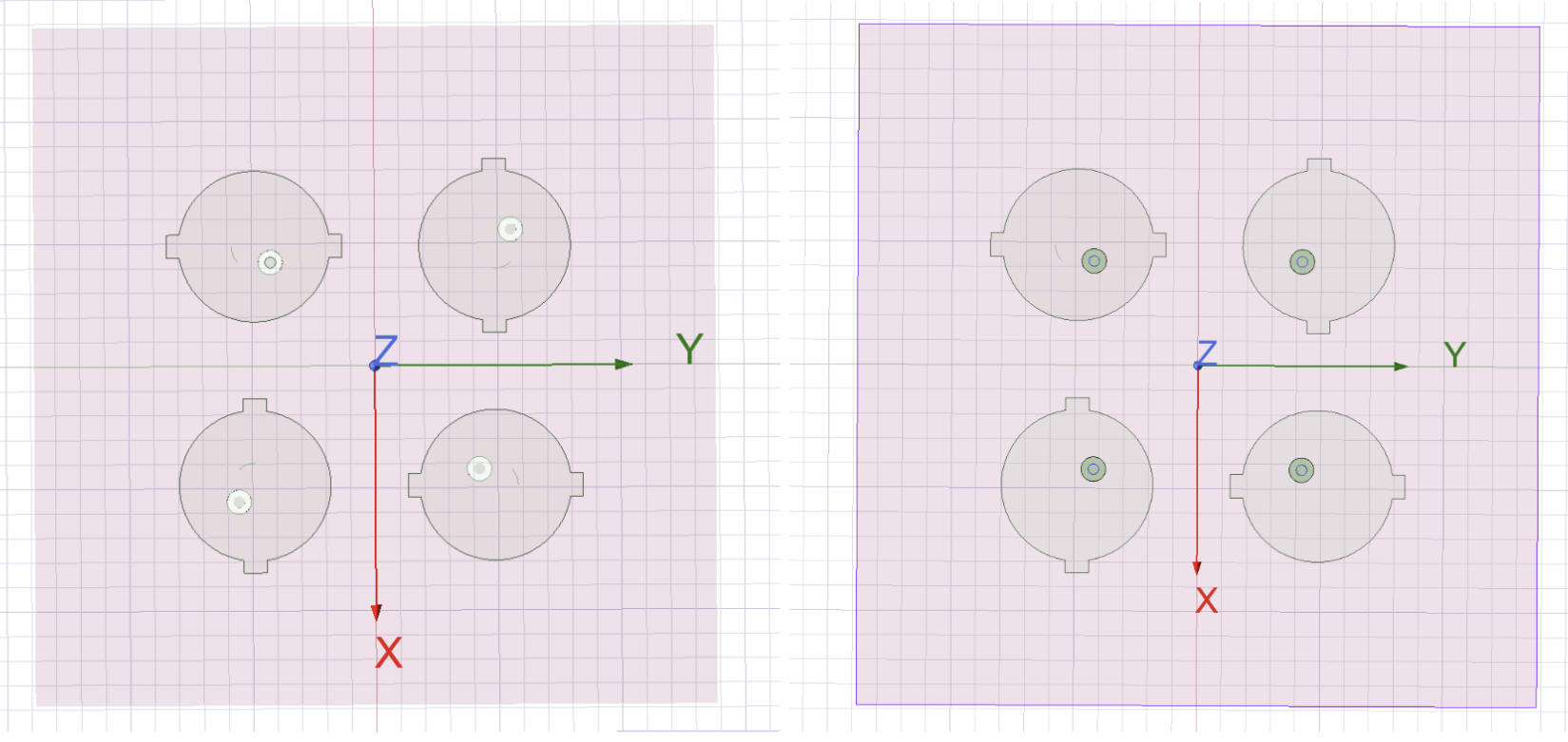
Figure 8. Effect of sequential rotation order on feed point position: (left) ‘diamond’ configuration, (right) ‘square’ configuration
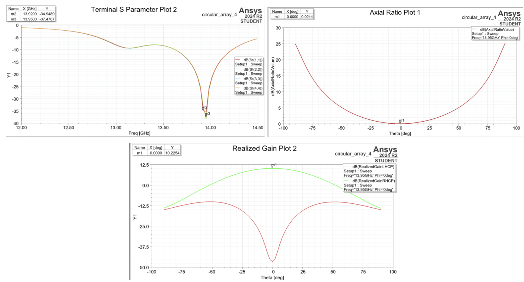
Figure 9. Performance comparison of different sequential rotation orders: a) S11, b) Axial Ratio, c) Realised Gain
| Metrics (boresight at 13.95 GHz) | Previous orientation | New orientation | Change |
|---|---|---|---|
| S11 | -35.5 dB | -37.5 dB | -2 dB |
| Realised RHCP Gain | 10.74 dBi | 10.23 dBi | -0.51 dBi |
| AR | 0.96 dB | 0.024 dB | -0.936 dB |
Table 5: Comparison of Sequential Rotation Orientations (Prototype 3)
The new orientation sees improvements in S11 and AR but worse gain. The better S11 is likely because when feed points are closer, the mutual impedance between feeds (vias) modifies the self-impedance of each patch, which in this case moves the impedance seen at each feed point closer to 50 Ohm (Mohammadian, Martin, & Griffin, 1989; Wang et al., 2010). However, mutual coupling also leads to worse radiation performance (gain). The improved AR is likely due to enhanced symmetry [Sequential Rotation of Antenna Array Elements Rotation Angle for Optimum Array Polarization Karsten Kuhlmann] of the ‘square’ over ‘diamond’ configuration. Due to improvements in S11 and AR, and minor loss in gain, this new orientation was chosen over the previous one.
4.4 Prototype 4: 2x4 Array Simulation
In the previous prototypes, the 2x2 arrays achieved gains of 10.74 dBi and 10.23 dBi respectively. This just meets our 10 dBi gain requirements. However, it is better to have a margin of 50% above 10 dB to account for losses from the feed network and manufacturing tolerances. Thus a safe target gain would be ~11.8 dBi. Hence, the 2x2 array was doubled to a 2x4 array, theoretically increasing gain from ~10 to ~13 dBi.
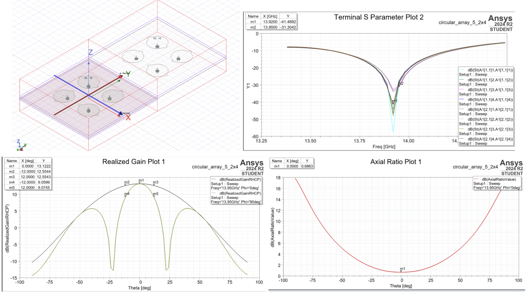
Figure 10. Performance of 2x4 Array (Prototype 4): a) Array geometry, b) S11, c) Realised Gain, d) Axial Ratio
| Metrics (boresight at 13.95 GHz) | Best achieved metric |
|---|---|
| S11 | -31.3 dB |
| Realised RHCP Gain (boresight) | 13.12 dBi |
| Realised RHCP Gain (+- 12 degrees) | 9.06 dBi |
| AR | 0.683 dB |
Table 6: 2x4 Array Simulation Metrics (Prototype 4)
The S11 and AR still satisfy our requirements very well. However, the radiation pattern is no longer similar from all orientations as the array is rectangular instead of square. The narrowest beamwidth taken at the phi=90 deg cut still satisfies our HPBW requirements as gain at +- 12 degrees is above 7 dBi.
4.5 Concept Selection: Feed network design
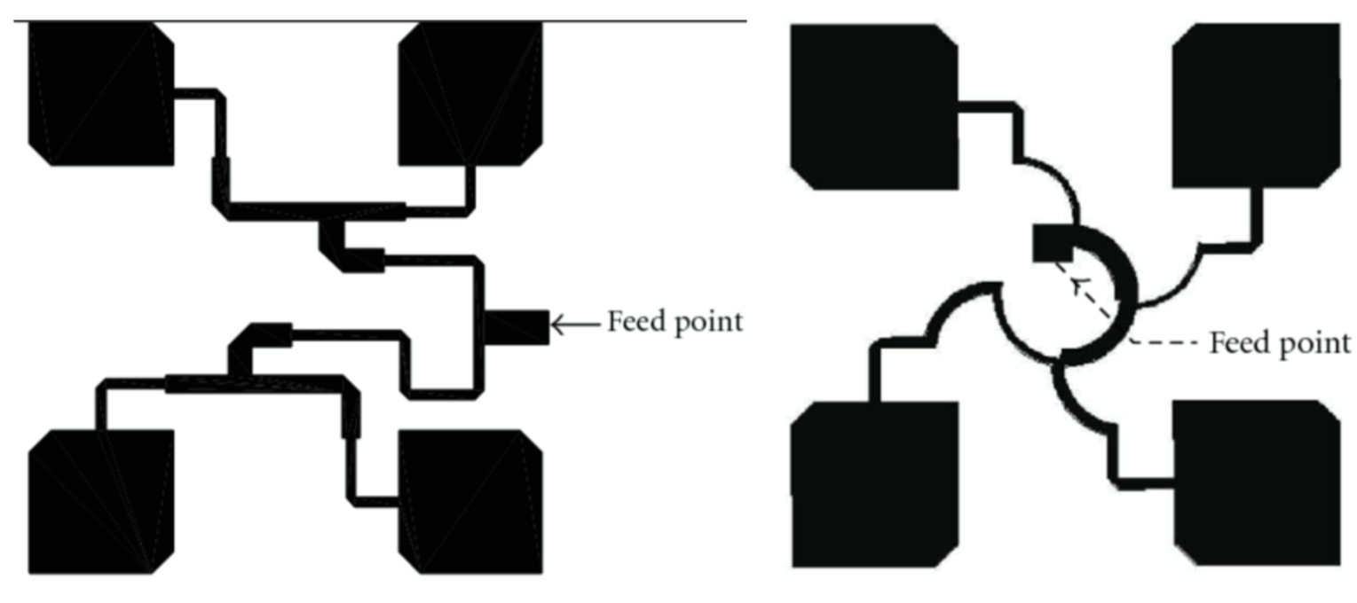
Figure 11. Feed Network Topologies: (left) Utilising T-junctions and 90-degree bends, (right) Sequentially rotated ‘arc’ network
Conventionally, feed networks utilise T-junctions. Every T-junction splits the power into two branches via quarter-wave transformers, to achieve the desired phase arrangement and power distribution (Chen et al., 2012). Keeping the resultant branches matched to the characteristic impedance of the source is crucial to minimising the S11. For simplicity of design, when change of direction is needed, 90-degree bends are utilised (Fig. x). However, for sequentially rotated arrays, a special ‘arc’ feed network can be utilised (Fig. x), offering a compact way to add a fixed length for each phase shift (Nezami, 2025).
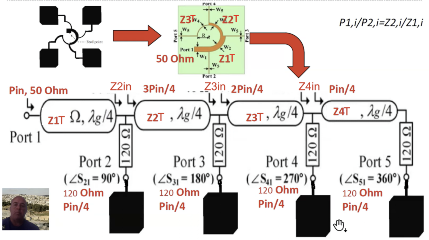
(Nezami, 2025)
Using power-splitting and quarter-wave transformer formulae (see Appendix x), one can calculate the microstrip line widths of each quarter-wavelength section of the ‘arc’ given the input impedance (50 Ohm), patch impedance (currently 50 Ohm but changeable if needed) and the lower substrate height, h2. The main check is to ensure the widths are neither too large nor too small as mentioned in 3.5.2.
Below are listed the key trace widths: Z1T to Z4T for a range of patch impedance Z_P and substrate height h2.
h2 is constrained to [0.686, 838], maximum 10% difference from h to reduce PCB warping (See 3.5). The quarter wavelength is calculated from the guided wavelength (from r and 0) to be 3.18mm.The minimum manufacturable trace width from PCB suppliers is 0.0508mm (PCBWay, n.d.). To limit crosstalk with other traces and feed points, and based on the standard separation for high frequency traces: 3-5 times the trace width (Sierra Circuits, n.d.), the maximum acceptable trace width can be calculated to be 1.09mm.
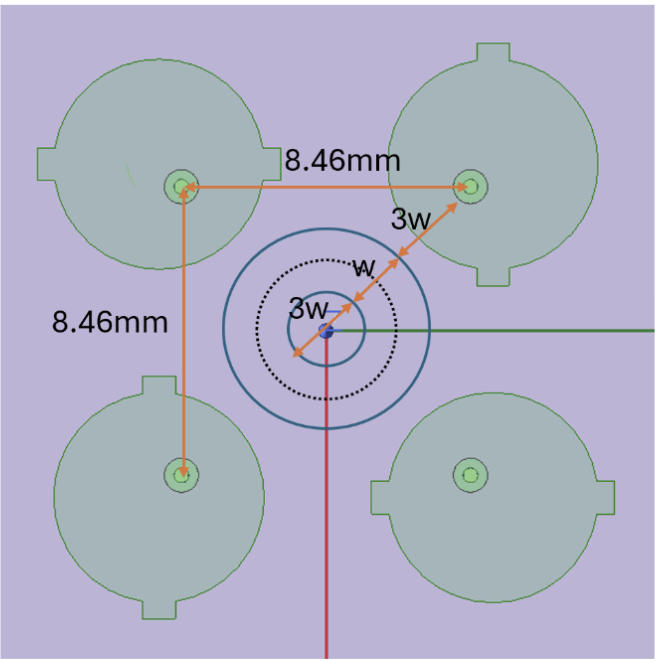
Figure x. Maximum acceptable trace width (in blue) calculation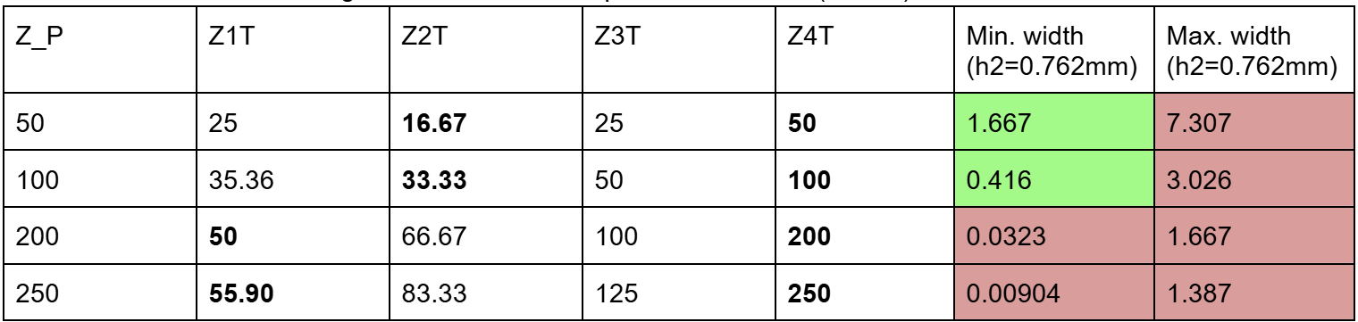
Table x.
As seen in Table x, in order to get a smaller maximum width, the minimum width will decrease much below the minimum manufacturable. Thus, the sequential rotated feed is not feasible given our compact patch arrangement.
Thus, the feed network will use the T-junctions and 90-degree bends.
4.6 Prototype 5: Feed network
4.6.1 Microstrip and T-junction simulations
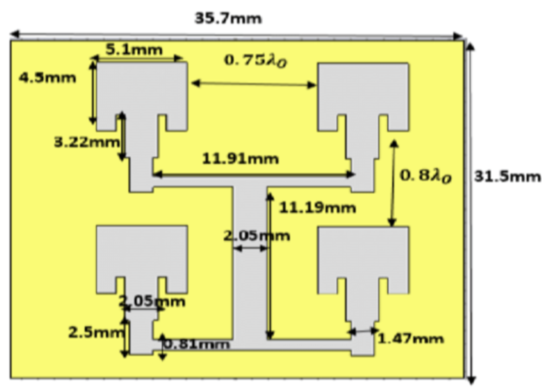
Figure 12. Typical microstrip feed network
Using the formula (source), I calculated the 50 Ohm microstrip width to be 1.1112mm for substrate height of 0.508mm. I simulated this microstrip line and found a very good S11 of -31.8 dB.
Using this trace width, I created the T-junction (Fig. x) which splits the power into two feeds of 50 Ohm characteristic impedance each. This is done by first splitting the starting feed (50 Ohm) to two 100 Ohm lines, each transformed via a quarter wavelength 70.7 Ohm line (Appendix for formula) to 50 Ohm.
Then, since there is limited space between the patch feed points, I hypothesised that 100 Ohm lines could be omitted and the result would be the same. So I simulated this case (Fig. x), found the reflection to be unacceptable at -13 dB. To solve this, I added mitered bends with tuned dimensions, (Fig. x) shown to help reduce losses (lit), reducing S11 to -35.6 dB.
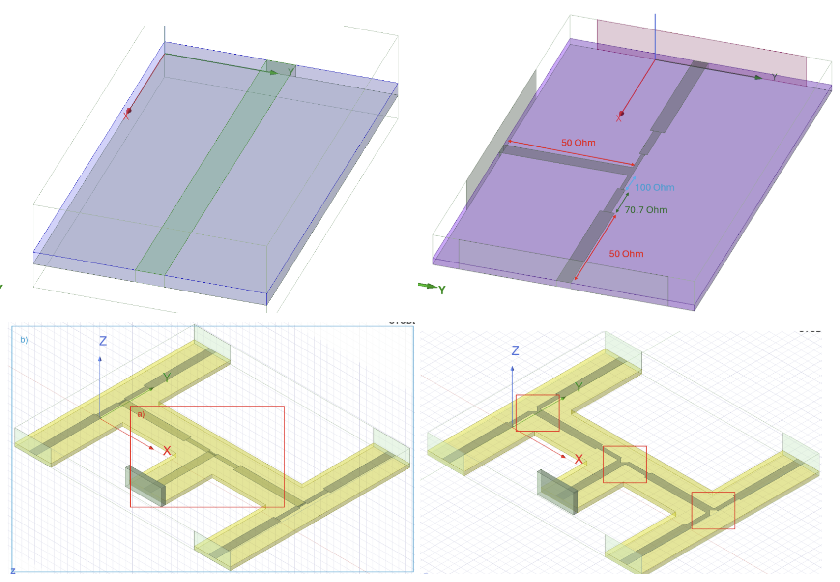
Figure 13. T-Junction Optimisation: (left) S11 comparison for T-junction without 100 Ohm line, (right) Mitered bends for T-junction to reduce losses
4.6.2 Design of Feeds with 90-degree Phase Shifts
The previously calculated quarter wavelength is the difference in feed length for each patch. Using this, the feeds for each patch are laid out with the appropriate lengths. It was hypothesised that even though some of the traces get closer than the 3-times width separation, that it occurred infrequently enough for the losses to be insignificant. After design, the phase shifts, S11, transmission coefficients (Sx1 representing S21 to S51, where 2-5 are the feed points while 1 is the source) and gain are evaluated.
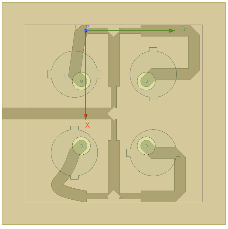
Figure x.
Unexpectedly, there were significant losses in the feed network which worsened the gain and AR. This was suspected due to the large difference in transmitted power, in which there was a ~2.3 dB (70% difference) in power transmitted to ports 2 and 5. Despite the strong focus on tuning the phase shifts, the neglect of the 3-times trace width separation rule was the main culprit behind these losses. To mitigate this issue, a mix of increasing the patch spacing and tuning h2 so traces can be narrower may be the solution.
4.7 Prototype 6: PCB v1
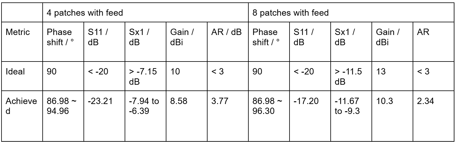
At this point, it was necessary to start fabrication for a functional prototype before the critical design review. The gain for 8 patches is now at 10.3 dBi. However, the target including a 50% margin is 11.5 dB. Thus, the array was doubled to 4x4. A gain of 13 dBi is expected, exceeding the target. For the gain at +- 12 deg, we will also target 8.5 dB, 50% above the required 7 dBi.
The final feed network (Fig. x) was created by copying the 2x2 subarray 4 times, with more T-junctions to feed each subarray from one source. An SMA connector footprint was also added on the feed layer for the power input. This design was simulated (Fig. x, Table x), all metrics satisfying the target, except the gain at +-12 degrees narrowly misses 8.5dB by ~0.2dB. This small variation was deemed acceptable as there is insufficient time to optimise it further.
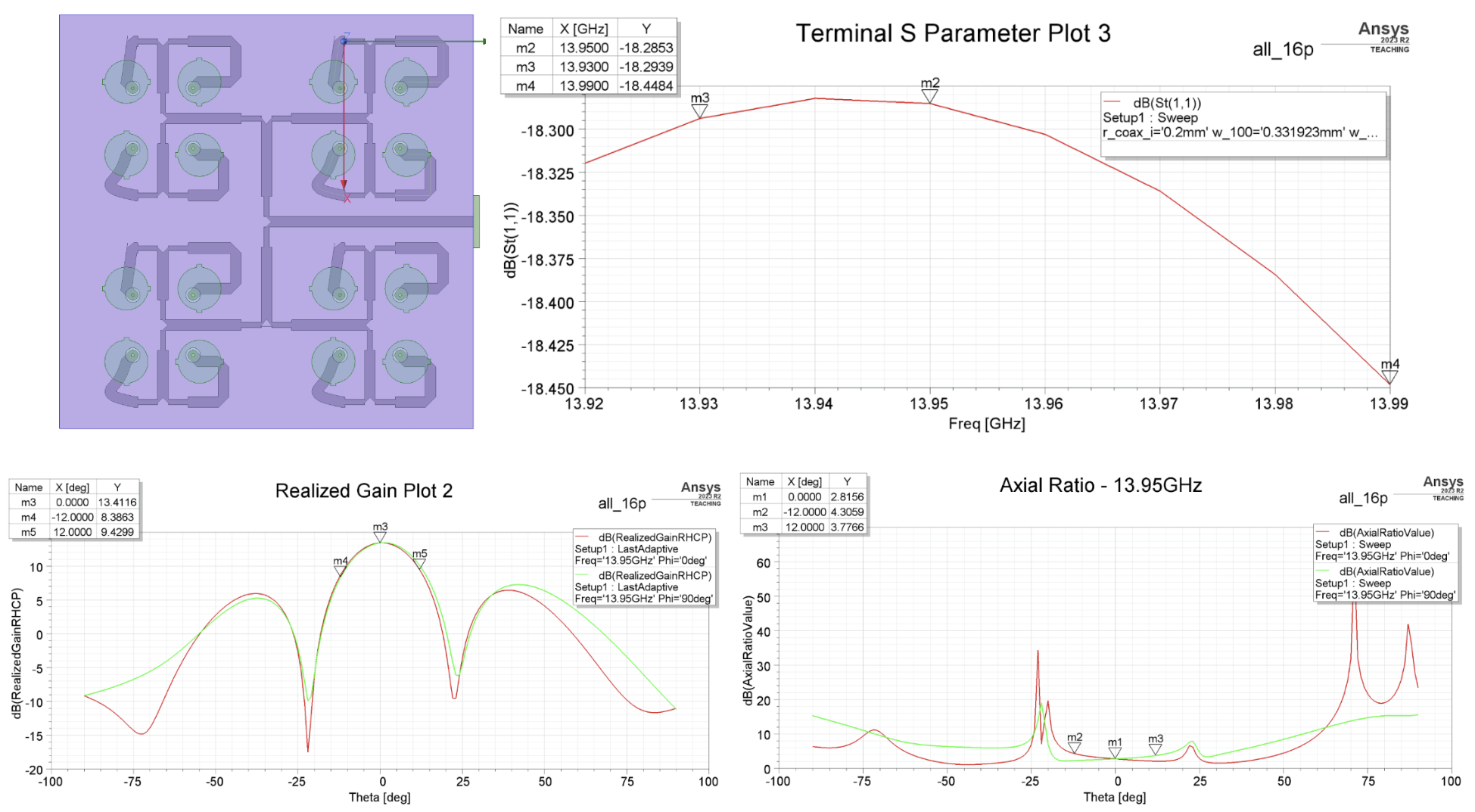
Figure x.
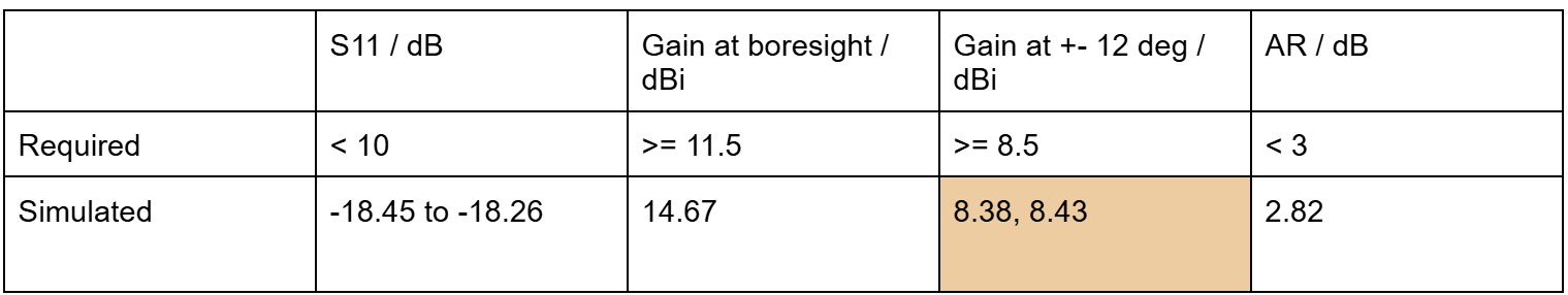
Table x.
To make the design fabrication-ready, an SMA footprint was added so power can be fed to the antenna via an SMA connector. The substrate dimensions were also expanded to 98mm x 98mm so that 4 mounting holes could be included. Thus, the design was fabricated by converting the HFSS file to Gerber and NC drill files via DipTrace, a PCB design software. The files were sent to PCB manufacturer PCBWay, who manufactured the prototype which will be referred to as PCB v1 from now.
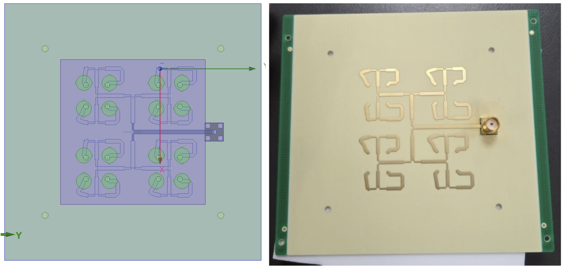
Figure x. a) Fabrication-ready design of antenna including mounting holes, SMA connector solder pad (left); b) Fabricated PCB bottom layer with soldered SMA connector (right). Note that a) shows the top-down view while b) shows the bottom view, thus why the feed network appears flipped.
4.7.1 Electrical Separation and Mechanical Stability
While the antenna was getting fabricated, it was noted that electrical separation is required between the bottom feed layer and other metal components of the CubeSat. For both electrical separation and mechanical stability, a Rohacell 31 HF foam will be added below the feed layer. It was simulated that a 12mm thick foam will be sufficient to prevent any metal in the back from affecting the key metrics. Thus, the foam was procured. Mounting holes and a hole for the SMA connector to be plugged in were drilled.
My NUS mentor also gave feedback that a central screw could be added for mechanical stability. As a central metal screw would be too close to the patches and feed traces, a plastic screw at similar dielectric constant to Rogers 4350B could be utilised. This will be done in the second fabricated design later.
5. Testing & Analysis
S11 measurement of the fabricated PCB v1 was done on a Vector Network Analyser (VNA) in the MMIC Lab and automated testing of key metrics was done at Temasek Labs’ anechoic chamber. These measured results were compared with the simulated S11.
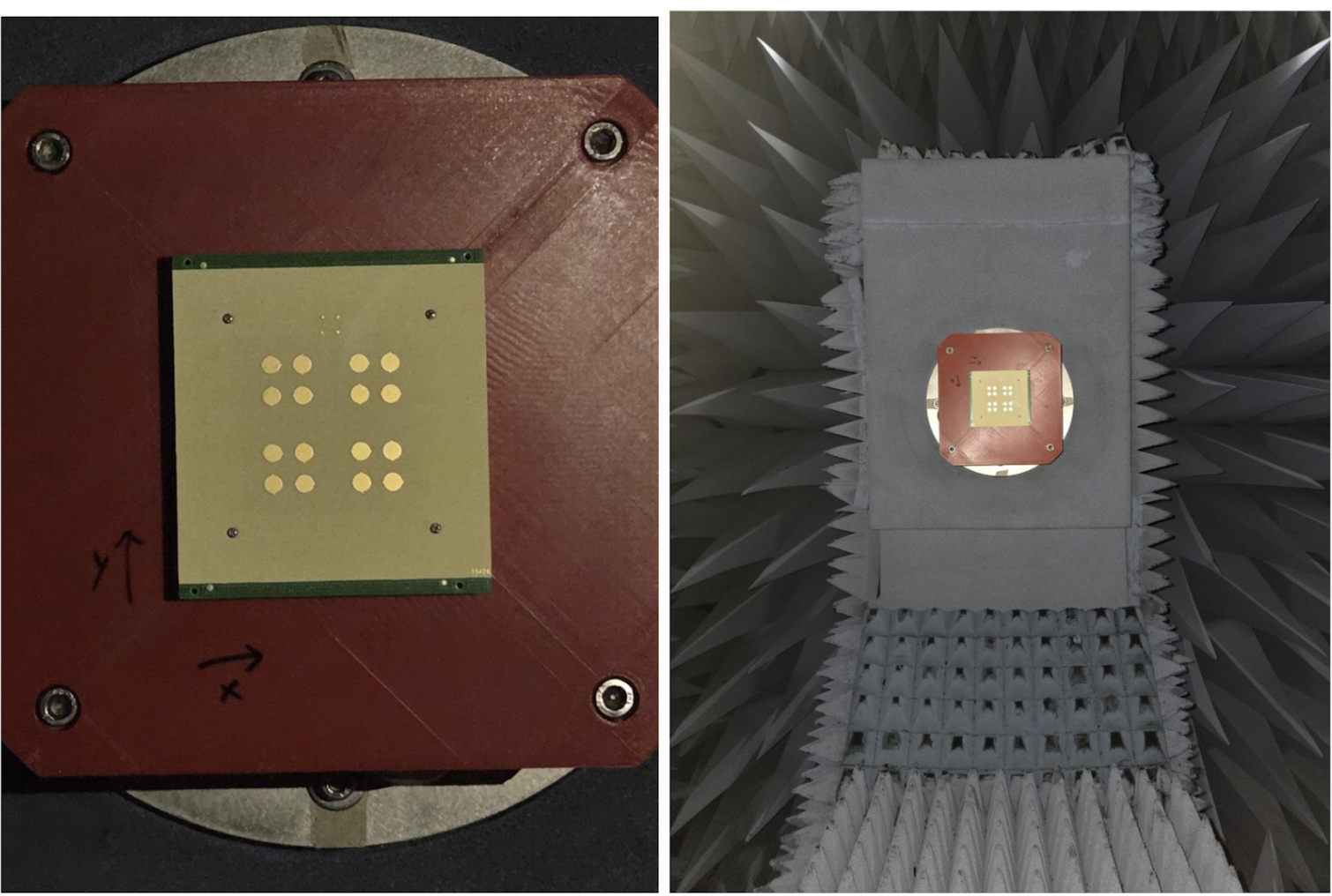
Figure x. Antenna mounting setup in the anechoic test chamber.
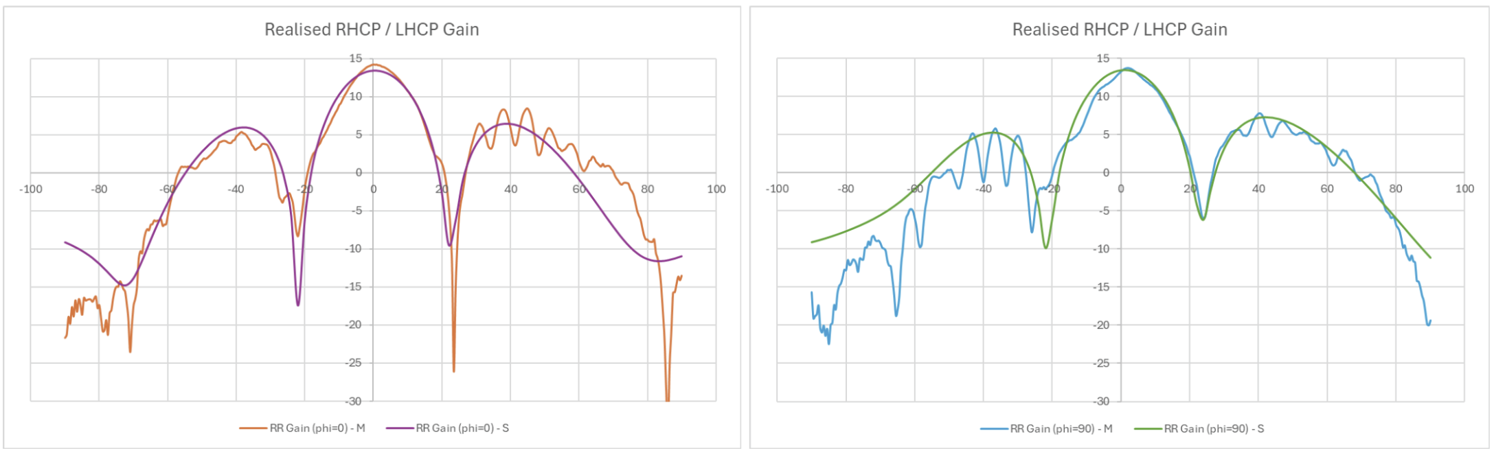
Fig x. Measured (M) vs. Simulated (S) Realised RHCP Gain for two x-axis cuts: phi = 0 and phi = 90 (see Appendix x)
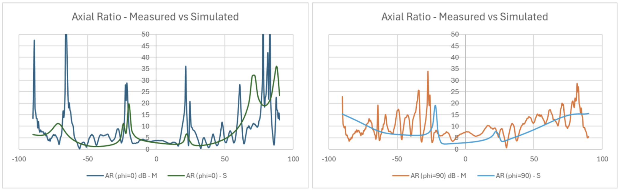
Fig x. Measured (M) vs. Simulated (S) Axial Ratio for two x-axis cuts: phi = 0 and phi = 90
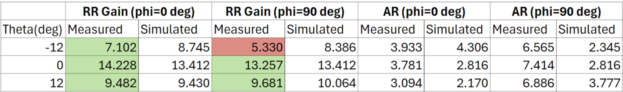
The measured gain is within 1-2 dB of the simulated values, which all satisfy requirements except the beamwidth at phi = 90 deg is too narrow, such that at -12 degrees, the gain is 1.7 dB short of the required 7 dB. After discussing with the team lead, this was found to be (?) acceptable.
For the AR, the AR at phi = 0 was within 1 dB of simulated values, but at 90 degrees, the AR was as high as 7.4 dB which was surprising.
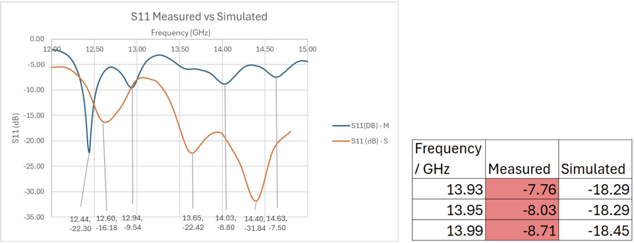
Fig x. Measured (M) vs. Simulated (S) S11, with minimums labelled; Table x. Measured (M) vs. Simulated (S) S11
The S11 shows a huge difference between simulation and measurement. Due to the many minimums present, it is hard to tell which minimums are which and whether they have shifted left or right from the simulation. Thus, generally, it can only be concluded that something had caused large power losses, most likely the feed network. In the frequency range of operation, the maximum S11 is -7.76 dB which is a power reflection of 16.8%.
Upon analysis, a key issue with PCB v1 was identified, which is that the simulations had not accounted for manufacturing tolerances in the feed network trace widths. Especially important are the widths of the 70.7 Ohm quarter-wave transformers, the narrowest traces in the PCB, as they determine the impedance matching with remaining parts of the feed and hence can cause large losses if their widths vary too much. In 4.6, the feed network simulation revealed that within a 2x4 array, the power delivered to each patch could vary as much as 70%. This issue, exacerbated by the 70.7 Ohm lines manufacturing tolerances, could have led to an even greater difference in power delivered to each patch, explaining why the AR to was greatly worsened.
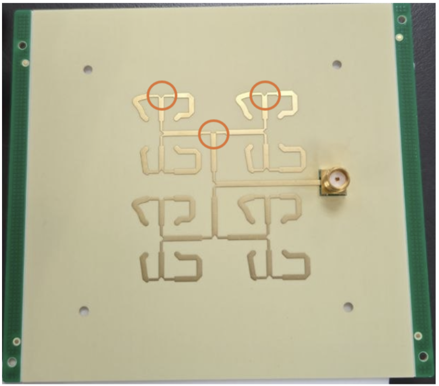
Fig x. Quarter-wave transformer lines (2 per T-junction), 3 out of many circled in orange
It is possible to simulate the manufacturing tolerances to check if the S11 and AR are worsened like in the measurement. According to PCBWay, for the 70.7 Ohm lines at width (w70) = 0.6878mm are controlled within 20%, which is +- 0.1376mm. For the minimum and maximum deviations, the antenna was resimulated. This verifies that indeed, the trace width tolerance of w70 could account for up to 7 dB of losses. The remaining 3dB of loss difference with the measured S11 can likely be attributed to trace tolerances for other lines such as the 50 Ohm line.
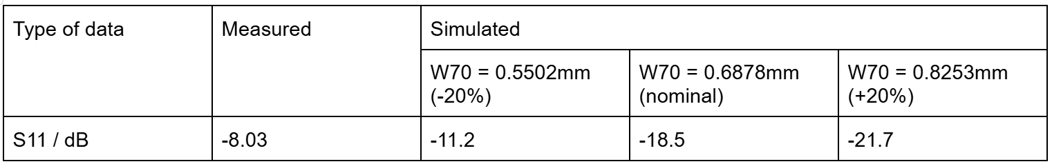
Table x.
6. Future Plans
To address the S11 performance and further optimise the antenna, the following future works are planned for PCB v2. The new design will strictly adhere to the 3-times trace width separation rule to eliminate crosstalk and transmission losses observed in the first iteration. Further tuning of h2 will be conducted to allow for narrower trace widths, facilitating greater electrical separation, especially between critical power-splitting junctions. However, the trace widths must also not be too narrow so as to cause large manufacturing tolerances. The tradeoffs between electrical separation and tolerances will be evaluated so as to choose an optimal h2 and trace widths. It is also possible to pay more (about $100 more for 4 PCBs) for PCBWay to control the trace widths within 10% instead of 20%, which also helps to decrease tolerance errors.
Furthermore, following mentor’s feedback, a central plastic screw will be integrated into the final assembly to enhance the mechanical stability of the three-layer stackup during launch vibrations without disrupting the electromagnetic fields.
7. Conclusion
This project successfully designed, simulated, and prototyped a custom Ku-band circularly-polarised microstrip patch array for the Galassia 5 CubeSat mission. By addressing the gap in commercially available space-qualified hardware for the 13.93-13.99 GHz range, this design provides a critical communication link for the satellite.The use of a 4x4 sequentially-rotated array was instrumental in achieving a high realised RHCP gain of 13 dBi, exceeding the initial design specifications. Although S11 deviations were observed due to feed network density, the project successfully validated the viability of a low-profile, ceramic-substrate antenna for high-frequency space applications.
8. References
Abulgasem, S., et al. (2021). Antenna designs for CubeSats: A review. IEEE Access, 9.
AL-Oqla, F. M., & Omar, A. A. (2015). An expert-based model for selecting the most suitable substrate material type for antenna circuits. International Journal of Electronics, 102(6), 1044–1055.
Amani, Y., & Zehforoosh, Y. (2016). Circularly polarised slot antenna for wireless applications. International Journal of Electronics, Mechanical and Mechatronics Engineering, 6(3), 1267–1274.
Arockia Michael Mercy, P., & Joseph Wilson, K. S. (2023). Bandwidth enhancement analysis of rectangular microstrip patch antenna for various substrates. PriMera Scientific Engineering, 2(5), 29–40.
Balanis, C. A. (1997). Antenna theory analysis and design. Wiley.
Chahat, N. (2021). CubeSat antenna design (1st ed.). IEEE Press / John Wiley & Sons, Inc.
Christopher, R. M., Uhl, B. H., & Jedlicka, R. P. (2004). Increasing polarisation bandwidth for single-layer, circularly-polarised microstrip patch antennas incorporating size reduction techniques. 2004 USNC/URSI National Radio Science Meeting.
Comparative study of microstrip patch antenna for microstrip feed line and different substrate. (2014). International Journal of Engineering Trends and Technology (IJETT), 7(2), 94–96.
Convergentia. (n.d.). Antenna design process.
Coonrod, J. (2010). General information of dielectric constants for circuit design using Rogers high frequency materials. Rogers Corporation.
Denker, R. (2025, July). All about circular polarisation and the axial ratio. Microwaves & RF.
Ezurio. (n.d.). Understanding antenna design.
Fan, F. F., Wang, W., Yan, Z. H., & Tan, K. B. (2014). Circularly polarised SIW antenna array based on sequential rotation feeding. Progress In Electromagnetics Research C, 47, 47–53.
FS PCBA. (2024). A one-stop solution for a variety of Rogers PCB materials.
GeeksforGeeks. (2023, November 29). Microstrip patch antenna. https://www.geeksforgeeks.org/microstrip-patch-antenna/
Gurbet, Y. S., & Doğu, S. (2025). Comprehensive review of Ku, K, and Ka band antenna designs: Applications in CubeSats. International Journal of Aeronautical and Space Sciences. https://doi.org/10.1007/s42405-025-00989-5
Hossain, M. A. (2023). Highly miniaturised and gain-enhanced ultra-wideband antennas for ground-penetrating radar systems [Doctoral dissertation, UC Davis].
Imbriale, W. A. (2003). Large antennas of the Deep Space Network. John Wiley & Sons, Inc.
Indharapu. (2022). Supervised machine learning model for accurate output prediction of various antenna designs. ResearchGate.
Intrasensors. (2024, October). Blog - Designing an antenna.
Jackson, D. R. (n.d.). Introduction to microstrip antennas. UH Cullen College of Engineering.
Kovitz, J. M., Santos, J. P., Rahmat-Samii, Y., Chamberlain, N. F., & Hodges, R. E. (2014). Development of a low-cost lightweight advanced K-band horn antenna with charge-programmed deposition 3D printing. IEEE Antennas and Propagation Magazine.
Kuhlmann, K. (2023). Sequential rotation of antenna array elements – rotation angle for optimum array polarisation. Advances in Radio Science.
Li, Q., et al. (2018). Research article: Mutual coupling reduction between patch antennas using meander line. International Journal of Antennas and Propagation.
MacroFab. (n.d.). PCB antenna design: A step-by-step guide.
MathWorks. (n.d.). Modeling & simulating antenna arrays and RF beamforming algorithms.
Minz, L., Kang, H., & Park, S. O. (2020). Low reflection coefficient Ku-band antenna array for FMCW radar application. Progress In Electromagnetics Research C, 102.
Mohamadzade, B., et al. (2020). Mutual coupling reduction in microstrip array antenna by employing cut side patches and EBG structures. Progress In Electromagnetics Research M, 89.
Mohammadian, A. H., Martin, N. M., & Griffin, D. W. (1989). A theoretical and experimental study of mutual coupling in microstrip antenna arrays. IEEE Transactions on Antennas and Propagation, 37(10), 1217–1223. https://ieeexplore.ieee.org/document/43529
Muludi, Z., & Budi, E. (2017). Truncated microstrip square patch array antenna 2 × 2 elements with circular polarisation for S-band microwave frequency. 2017 International Electronics Symposium (IES). https://doi.org/10.1109/elecsym.2017.8240384
NASA. (n.d.). Small spacecraft technology state of the art report: Communications.
Nema, R., & Khan, A. (2012). Analysis of five different dielectric substrates on microstrip patch antenna. International Journal of Computer Applications, 55(18), 0975–8887.
(Nezami, 2025) https://youtu.be/FdIyejhALto?si=LUkd-kc3n_ZUSGRz
Nguyen-Huy, H., Tran, H., Pham-Duy, H., Dao-Duc, T., & Hussain, N. (2026). Compact and low cross-polarisation microstrip patch antenna for 5G Internet of Things applications. PLoS One, 21(2), e0341549.
Pasternack. (2019). Microstrip patch antenna calculator. https://www.pasternack.com/t-calculator-microstrip-ant.aspx
Paul, L. C., Hosain, M. S., Sarker, S., Prio, M. H., Morshed, M., & Sarkar, A. K. (2015). The effect of changing substrate material and thickness on the performance of inset feed microstrip patch antenna. American Journal of Networks and Communications, 4(3), 54–58.
PCBSync. (n.d.). Microwave PCB design: Choosing the right substrate.
Ray, I., Khan, M., Mondal, D., & Bhattacharjee, A. K. (2008). Effect on resonant frequency for E-plane mutually coupled microstrip antennas. Progress In Electromagnetics Research Letters, 3, 133–140.
Richa, N., Sharma, M. M., Sharma, I. B., Jaiverdhan, Kaith, P., & Garg, J. (2021). Design and performance evaluation of circularly polarised dual feed microstrip patch antenna using Wilkinson power divider. 2021 IEEE Indian Conference on Antennas and Propagation (InCAP), 12–14. https://doi.org/10.1109/incap52216.2021.9726355
Rogers Corporation. (n.d.). RT/duroid 5870 - 5880 data sheet.
Rolo, M. (2022). Planar antennas for CubeSat missions electronics engineering. ISTsat.
Saeidi, T., & Karamzadeh, S. (2025). Enhancing CubeSat communication through beam-steering antennas: A review of technologies and challenges. Electronics, 14.
Shah, V. A., & Patel, R. N. (n.d.). Substrate material effect on MPA design parameters. Indian Journal of Applied Research.
Silva, W., Campos, A., & Guerra, J. (2021). A compact dual-band UHF microstrip patch antenna for CubeSat applications. Journal of Communication and Information Systems, 36(1), 166–172. https://doi.org/10.14209/jcis.2021.18
Sowmya, M., Narayana, M. V., Govardhani, I., & Khan, H. (2012). Design of a ultra wide-band capacitive feed microstrip patch antenna for Ku-band applications. International Journal of Current Research and Review, 4(14).
Tubbal, F., Raad, R., & Chin, K. W. (2015). Antenna designs for CubeSats: A review. IEEE Access, 3.
Veera, K. B., & Ajay, K. D. (2025). Micro strip patch antenna utilization in cube satellite systems. i-manager’s Journal on Communication Engineering and Systems, 14(1), 28. https://doi.org/10.26634/jcs.14.1.21605
Verwilligen, W. (2015). A novel planar antenna for CubeSats. DigitalCommons@USU.
Zhang, J. (2011). Antenna miniaturisation in complex electromagnetic environments: Designs and measurements of electrically small antennas for hearing-aid applications [Doctoral dissertation, Technical University of Denmark].
Zhu, J., & Liu, J. (2025). Design of microstrip antenna integrating 24 GHz and 77 GHz compact high-gain arrays. Sensors, 25(2).
Zvolensky, T. (2022). Antenna radiation efficiency. rfe Blog.
Acknowledgements
I would like to thank my DSO mentor Ms Huang Ying Ying and my NUS supervisor Mr Chua Tai Wei, both with extensive knowledge on antenna design, whose guidance without which I would not have been able to complete my design tasks this semester. I would also like to thank my NUS supervisor Mr Eugene Ee and Mr Ng Zhen Ning from Nuspace for the practical and valuable advice they have offered that help in the realisation of this project.
9. Appendix
Appendix A: Detailed Performance Metric Definitions
S11 (Return Loss) is the ratio of reflected voltage to source voltage. A lower S11 is desired because a small S11 value indicates that a significant amount of energy has been successfully delivered to the antenna rather than being reflected back to the source due to a mismatch (Ezurio, n.d.). Ideally, the antenna and source impedance should match at the standard 50 Ohms. The standard is to ensure >90% power transmission, corresponding to S11 ≤−10 dB (Verwilligen, 2015) in the operational range of 13.93-13.99 GHz.
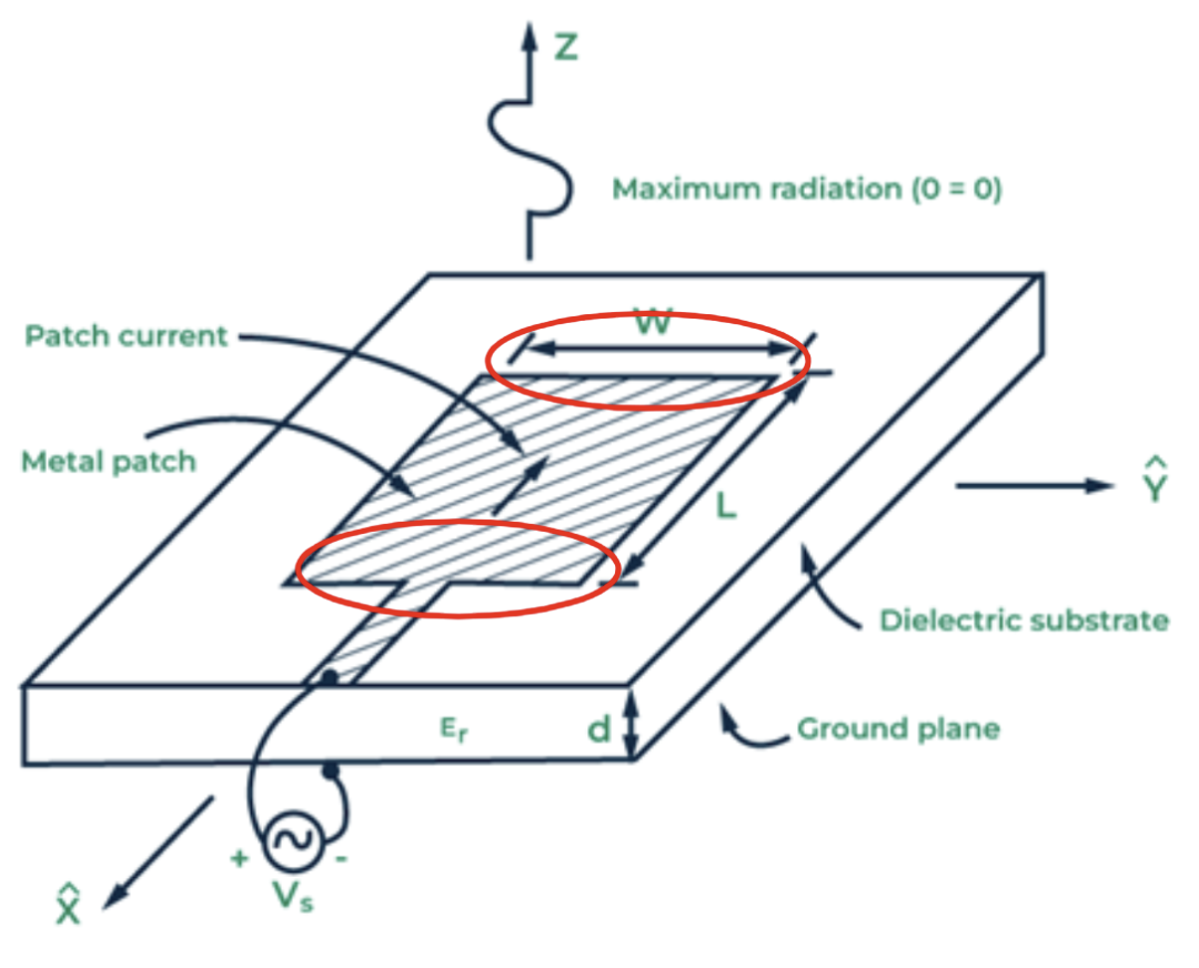
Figure 2. S11 (dB) vs Frequency
Polarisation is the direction in which the vibrations of the electromagnetic wave are restricted. To prevent signal attenuation and mitigate the atmospheric “Faraday rotation” effect, CubeSat antennas typically employ circular polarization (CP), making the communication link insensitive to antenna misalignment (Tubbal et al., 2021). Typically, right-hand circular polarisation (RHCP) is chosen for satellite communications to maintain a robust and properly aligned link with the ground station.
Gain describes how effectively the antenna concentrates radiated power in a particular direction compared to an isotropic radiator. A higher gain indicates a more focused beam. Realised RHCP Gain is a comprehensive metric that determines the true operating performance of the antenna because it includes the impedance mismatch at the feed port on top of the internal material and dielectric losses (Zvolensky, 2022), and the polarization mismatch (Denker, 2025). Thus, the realised RHCP gain at boresight will have to be ≥10 dBi.
Half-power beamwidth (HPBW) is the angle where the radiated power drops to half (−3 dB) of the boresight peak power. It describes how wide or narrow the beam is. For an antenna satisfying 10 dBi gain and +-12 degrees HPBW, the gain will need to be >=7 dBi at +-12 degrees.
Axial ratio (AR) defines the quality of the circular polarization by calculating the magnitude ratio of the electromagnetic wave’s two orthogonal, 90-degree phase-shifted field vectors (Kuhlmann, 2023). It measures the polarization purity of the wave; ideally, the AR must stay below 3 dB to ensure high-quality circular polarization (Abulgasem et al., 2021). Since our system strictly utilises RHCP without LHCP receivers, AR is not so significant as realised RHCP gain, and is just a measure of polarisation efficiency. If two antennas share the same realised RHCP gain, they yield identical received power, but the one with a higher AR wastes some of the source energy in unutilised LHCP cross-polarisation (Denker, 2025).
Appendix B: How the Circularly-Polarised Patch Antenna Works
The patch antenna consists of a conducting patch layered on top of a dielectric substrate, which is on top of a conductive ground plane. Through a feedline, alternating electric fields are formed between the patch and ground plane, which resonate and escape through both ends of the patch antenna which act as radiating slots (Jackson, n.d.; Orban & Moernaut, 2005).
Figure 3. Basic rectangular patch antenna [6]
To achieve circular polarisation, the antenna must simultaneously excite two orthogonal resonant modes (e.g., the TM10 and TM01 modes) with equal amplitude and a 90-degree phase difference (Helit Team, n.d.; Orban & Moernaut, 2005).